Home / Business and Economy / Odisha Lands India's First 3D Glass Chip Packaging Unit
Odisha Lands India's First 3D Glass Chip Packaging Unit
19 Apr
Summary
- India's first advanced 3D glass chip packaging unit started in Bhubaneswar.
- The project involves an investment of Rs 1,943 crore.
- It is expected to create over 2,500 direct and indirect jobs.
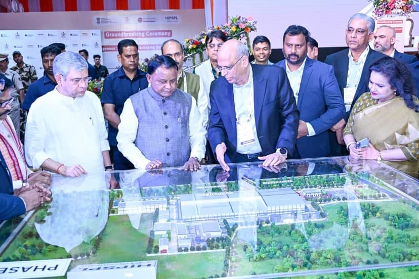
Heterogeneous Integration Packaging Solutions Pvt Ltd (3D Glass Solutions) has initiated construction on India's first advanced 3D glass chip packaging facility in Bhubaneswar. This project, representing an investment of approximately Rs 1,943 crore, was approved under the India Semiconductor Mission in August 2025 and is poised to boost Odisha's standing as a center for cutting-edge chip technology.
The facility is projected to produce around 50 million assembled semiconductor units each year, significantly enhancing India's chip packaging capabilities. Backed by US technology, the unit will focus on glass-based RF and millimetre-wave packaging substrates, enabling high-performance computing, AI, and IoT applications. This initiative is a crucial step in India's semiconductor roadmap, aiming to reduce import reliance and foster domestic innovation.
Chief Minister Mohan Charan Majhi and Union Electronics and IT Minister Ashwini Vaishnaw attended the foundation stone-laying ceremony. The project is anticipated to create over 2,500 jobs, signaling Odisha's strategic shift towards high-value manufacturing and advanced technology sectors, moving from a mineral-driven economy to a mind-driven one.