Home / Technology / US-Made 3D Chip Redefines AI Hardware
US-Made 3D Chip Redefines AI Hardware
24 Dec, 2025
Summary
- New 3D chip architecture offers order-of-magnitude performance boost.
- Monolithic 3D integration built in a commercial U.S. foundry.
- Addresses AI's 'memory wall' and 'miniaturization wall' challenges.
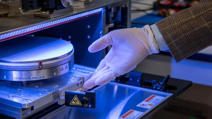
Engineers from leading U.S. universities have collaborated with SkyWater Technology to develop a novel multilayer computer chip architecture. This vertically integrated 3D design stacks components like floors in a building, utilizing vertical wiring for rapid data transfer. It significantly reduces the data bottlenecks plaguing conventional 2D chips, which struggle with the immense data demands of modern AI models.
The "monolithic" 3D integration approach builds each layer directly atop the previous one in a continuous process. This method, conducted within a commercial U.S. foundry, allows for tighter packing and denser connections than stacking separate chips. This domestic production capability is seen as crucial for U.S. semiconductor innovation, moving advanced chip concepts from academic labs to scalable manufacturing.
In hardware tests, the prototype demonstrated performance gains of approximately four times compared to 2D chips, with simulations predicting up to twelve-fold improvements for AI workloads. Beyond speed, the architecture offers a path to substantial energy efficiency gains, critical for future AI hardware development. This breakthrough signifies a new era for chip production and innovation within the United States.