feedzop-word-mark-logo
searchLogin
Feedzop
homeFor YouIndiaIndia
You
bookmarksYour BookmarkshashtagYour Topics
Trending
Terms of UsePrivacy PolicyAboutJobsPartner With Us

© 2026 Advergame Technologies Pvt. Ltd. ("ATPL"). Gamezop ® & Quizzop ® are registered trademarks of ATPL.

Gamezop is a plug-and-play gaming platform that any app or website can integrate to bring casual gaming for its users. Gamezop also operates Quizzop, a quizzing platform, that digital products can add as a trivia section.

Over 5,000 products from more than 70 countries have integrated Gamezop and Quizzop. These include Amazon, Samsung Internet, Snap, Tata Play, AccuWeather, Paytm, Gulf News, and Branch.

Games and trivia increase user engagement significantly within all kinds of apps and websites, besides opening a new stream of advertising revenue. Gamezop and Quizzop take 30 minutes to integrate and can be used for free: both by the products integrating them and end users

Increase ad revenue and engagement on your app / website with games, quizzes, astrology, and cricket content. Visit: business.gamezop.com

Property Code: 5571

Home / Science / New Laser Patterning Speeds Heat Control

New Laser Patterning Speeds Heat Control

18 Jan

•

Summary

  • Ultrafast lasers create nanoscale surface structures on silicon films.
  • Method controllably alters how heat moves through chip materials.
  • Process is over 1000x faster than electron-beam lithography.
New Laser Patterning Speeds Heat Control

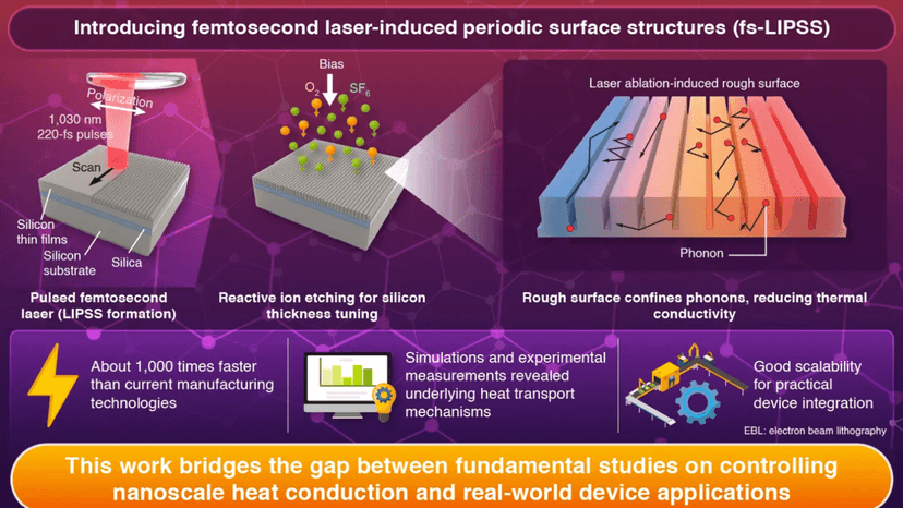
Engineers in Japan have devised an innovative technique that utilizes ultrafast laser pulses to modify the thermal properties of silicon and silica films at the nanoscale. By creating precisely spaced grooves on material surfaces, the method controllably alters how heat travels through electronic components, moving beyond traditional heat removal strategies.

This femtosecond laser-induced periodic surface structure (fs-LIPSS) process achieves nanoscale resolution at speeds more than 1000 times faster than single-beam electron-beam lithography. It is maskless, resist-free, and scalable for wafer-level implementation, aligning with current CMOS manufacturing standards and enhancing mechanical robustness.

The advancement holds significant promise for high-performance computing, quantum devices, and thermal management in dense GPU clusters for AI. Wider adoption will hinge on industrial-scale reproducibility, long-term stability, and cost-effectiveness, paving the way for more efficient electronics.

trending

Djokovic chases 25th Grand Slam

trending

Prince Albert medical procedure

trending

Draymond Green texted draft targets

trending

Australian Open Sinner, Alcaraz Dominate

trending

India vs New Zealand decider

trending

India vs New Zealand decider

trending

Courtney Walsh joins Zimbabwe

trending

JioHotstar entertainment watch time grew

trending

Shadowfax Technologies IPO opens

trending

BCB requests group swap

Disclaimer: This story has been auto-aggregated and auto-summarised by a computer program. This story has not been edited or created by the Feedzop team.
They use ultrafast lasers to create nanoscale patterns on silicon and silica films, altering phonon movement and thus thermal conductivity.
The fs-LIPSS process is over 1000 times faster while still achieving nanoscale resolution, making it more industrially relevant.
It's applicable to high-performance computing, quantum devices, and thermal management challenges in AI hardware and data centers.

Read more news on

Scienceside-arrow

You may also like

ASML's $400M Machine: The AI Economy's Heartbeat

4 Jan • 104 reads

article image

AMD Soars on AI Chip Demand Surge

3 Jan • 67 reads

article image

Palantir Soars: AI Hype Meets Real Demand

3 Jan • 98 reads

Quantum Stocks: Boom to Bust in 2025?

30 Dec, 2025 • 85 reads

article image

Quantum Computing Surges: Billions Flow In

23 Dec, 2025 • 107 reads

article image